Samsung is reportedly working on a next-generation mobile memory packaging approach called Multi Stacked FOWLP, according to a new report from South Korean outlet ETNews. If it reaches commercial products, the technology could raise memory bandwidth by roughly 15% to 30% while also increasing stack capacity by more than 1.5 times.
The report says this new design builds on Samsung’s existing vertical copper stack, or VCS, technology. The goal is to push past some of the long-standing limits found in traditional LPDDR packaging by using copper pillars with a much higher aspect ratio, which should allow more connection points in the same footprint.
In conventional mobile memory packaging, wire bonding is still common, and that tends to keep I/O terminal counts in the rough range of 128 to 256. It also comes with tradeoffs in signal loss, thermal behavior, and power efficiency. Samsung’s updated approach reportedly continues down the same general path as VCS, but makes the copper pillars thinner and taller so more interconnects can fit into tight spaces.
More specifically, the company is said to be targeting a major shift in pillar geometry, moving from an aspect ratio of around 3–5:1 to roughly 15–20:1. That change is expected to improve overall memory bandwidth, but it also creates a manufacturing problem: once those copper pillars become thinner than 10 micrometers, they can bend or even break more easily.
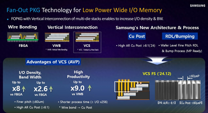
To address that, Samsung is reportedly combining the structure with fan-out wafer-level packaging. In practice, that means routing wiring outward after the chip is packaged so the extremely fine copper pillars get additional structural support. If the implementation works as described, the result would be a denser package with more I/O terminals in the same area.
That could matter for future phones and XR hardware, especially as local AI workloads become heavier and demand more from the memory subsystem. The article does note that no benchmark conditions were provided, so the projected gains shouldn’t be treated as a direct real-world user experience uplift just yet.
For now, the technology is still said to be under development, and there’s no confirmed mass-production or commercialization timeline. Some industry observers believe it could first appear alongside Exynos 2800 or possibly Exynos 2900, but that remains speculative at this stage.